Choosing a DDR Memory Controller for ASIC, FPGA, Automotive and Aerospace
A DDR memory controller is one of the highest-risk, highest-value blocks in any modern SoC. It sits on the critical path for bandwidth, latency and power, and its correct operation depends on a tight marriage between digital logic (the memory controller) and mixed-signal circuitry (the DDR PHY). Picking the wrong controller class — or misjudging ranks, ports, ECC or the PHY interface — can cost a full silicon respin or a failed functional-safety assessment. This guide gives the engineering depth needed to choose correctly across four very different targets: custom ASIC, FPGA, automotive and aerospace/defense.
Key Takeaways
- How JEDEC DDR terminology — channel, rank, bank group, chip select, DQ/DQS — maps to real electrical loading and timing.
- Why ranks are defined by chip selects, and how single/dual/quad rank affect capacity, timing (tRRD, tWTR, rank-to-rank turnaround) and signal integrity.
- How multi-port controllers arbitrate CPU, GPU, DMA, display and NPU traffic using QoS, reordering and coalescing.
- What the DFI (DDR PHY Interface) is, why JEDEC decoupled controller from PHY, and how training crosses the DFI boundary.
- A target-by-target selection method — ASIC vs FPGA vs automotive (ISO 26262) vs aerospace (rad-hard/EDAC) — with a decision flowchart.
- How to compute peak bandwidth: BW = data_rate x bus_width, with DDR4/DDR5 worked examples.
DDR Memory Terminology You Must Know
Before you can compare controllers you must speak the language of the JEDEC DRAM standard. These terms describe a strict physical and logical hierarchy. Getting them right is the difference between a controller that trains first time and one that fails at the board level.
Channel
A channel is an independent data path between the controller and DRAM, with its own command/address (CA) bus and its own DQ data bus. Each channel operates in parallel, so bandwidth scales with channel count. A DDR4 channel is 64 bits wide (72 with ECC). DDR5 splits a 64-bit DIMM into two independent 32-bit sub-channels (40 bits with ECC each), which improves efficiency for small bursts because each sub-channel has its own CA bus.
Rank
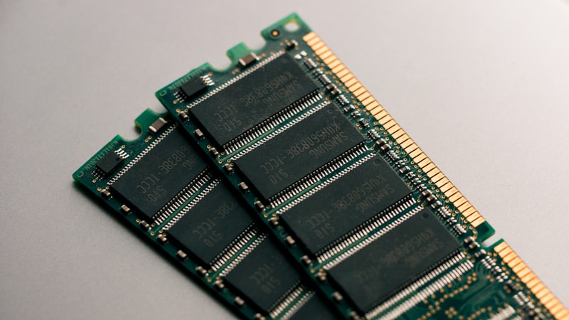
A rank is a set of DRAM chips that respond together to a single chip select and collectively drive the full channel data width. All DRAMs in a rank share the CA bus and the DQ bus but are enabled as a group. A rank is the unit of capacity you add to a channel without adding wires — you add a chip select instead. More ranks on a channel means more capacity but more electrical load on the shared DQ/DQS and CA nets.
Bank and Bank Group
Inside each DRAM die, storage is divided into banks, each an independent array with its own open row (page). DDR4 has 16 banks organized into 4 bank groups of 4 banks; DDR5 has 32 banks in 8 bank groups. Bank groups exist because accesses to different bank groups can be issued back-to-back faster (short column-to-column delay, tCCD_S) than accesses within the same bank group (tCCD_L). A good controller interleaves addresses across banks and bank groups to hide tRC/tRP/tRCD and keep the data bus busy.
Chip Select (CS)
The chip select (CS_n) enables one rank for a command. The number of CS lines a controller drives equals the number of ranks it can address per channel. This is the key relationship: rank count = chip-select count. A dual-rank channel uses CS0_n and CS1_n; the controller must manage rank-to-rank turnaround bubbles when switching the DQ bus ownership between ranks.
Row / Column
Within a bank, data is addressed by row and column. An ACTIVATE command opens a row into the bank's sense-amp row buffer (tRCD before a column access is legal); READ/WRITE commands then select a column. A PRECHARGE closes the row (tRP) before a different row in the same bank can be opened. Row-buffer hit rate is a first-order driver of effective latency and power.
DQ / DQS / DM
DQ are the bidirectional data bits. DQS is the source-synchronous strobe that clocks data in and out — center-aligned for writes, edge-aligned for reads, which is why read/write training and per-bit deskew exist. DM (data mask, or DM/DBI in DDR4+) enables partial writes and data-bus inversion to limit simultaneous switching. Each byte lane (8 DQ) has its own DQS pair for independent timing.
Command/Address (CA) Bus
The CA bus carries commands and addresses from controller to DRAM. DDR4 uses a wide multiplexed scheme; DDR5 and LPDDR use narrower, higher-speed CA buses (LPDDR5 uses a 7-bit CA) often with on-die command/address parity and, in DDR5, a dedicated per-command CRC option. CA bus integrity directly limits the maximum data rate on heavily loaded (multi-rank) channels.
| Term | Definition | Selected By | Impact |
|---|---|---|---|
| Channel | Independent CA + DQ data path | Controller port mapping | Parallel bandwidth |
| Rank | DRAM group driven by one CS | Chip Select (CS_n) | Capacity, loading, turnaround |
| Bank Group | Cluster of banks (tCCD_L domain) | BG address bits | Back-to-back access rate |
| Bank | Independent array with one open row | Bank address bits | Parallelism, row-hit rate |
| Row/Column | Page + offset within a bank | ACTIVATE / READ-WRITE | Latency (tRCD, tRP), power |
| DQ/DQS/DM | Data, strobe, mask/DBI | PHY byte lanes | Training, SI, max data rate |
Ranks Explained
Ranks are the most commonly misunderstood DDR concept, yet they drive capacity planning, timing budgets and signal integrity simultaneously. Remember the anchor: one rank = one chip select = one full channel-width group of DRAMs.
Single, Dual and Quad Rank
- Single rank (1R): One CS. Lightest DQ/CA load, highest achievable data rate, lowest capacity.
- Dual rank (2R): Two CS (CS0/CS1). Doubles capacity and enables rank interleaving to hide refresh and precharge, but adds a second electrical load on the shared data nets.
- Quad rank (4R): Four CS. Maximum capacity per channel but the heaviest load; usually requires registered/buffered DIMMs (RDIMM/LRDIMM) and often forces a lower data rate for signal-integrity margin.
Rank Interleaving
With multiple ranks, the controller can issue a command to rank 1 while rank 0 is busy with a refresh (tRFC), a precharge, or recovering from a write. This rank interleaving raises data-bus utilization — but only if the scheduler is rank-aware and the turnaround penalty is paid intelligently.
Capacity, Loading and Timing
Each rank you add multiplies capacity but also multiplies the capacitive and ISI load on DQ/DQS and the CA bus, which is why multi-rank channels frequently de-rate: a single-rank channel may run DDR4-3200 while a quad-rank channel on the same board runs DDR4-2133. Key rank-sensitive timing parameters the controller must honor:
- tRRD_S / tRRD_L: ACTIVATE-to-ACTIVATE delay to different / same bank group.
- tWTR_S / tWTR_L: internal write-to-read turnaround, short (different bank group) and long (same bank group).
- Rank-to-rank turnaround: a dead cycle (bus idle "bubble") inserted when DQ bus ownership moves from one rank to another so drivers do not collide; this grows with data rate.
- tFAW: four-activate window limiting how many rows can open in a rolling time span (a power/current constraint).
Multi-Port Memory Controllers
A single DRAM channel has one physical data bus, yet a modern SoC has many masters that all need it: the CPU cluster, GPU, display controller, camera/ISP DMA, networking, and increasingly an NPU for ML inference. A multi-port memory controller presents several independent ports (typically AXI/CHI) to these masters and multiplexes them onto the shared DRAM channel while meeting each master's bandwidth and latency contract.
Why Multiple Ports
Different masters have fundamentally different traffic profiles. The CPU is latency-sensitive (small, random, blocking reads). The GPU and NPU are bandwidth-hungry and latency-tolerant. The display engine is isochronous — it must never underrun or the screen tears, so it needs a guaranteed-bandwidth, bounded-latency contract. A single arbiter has to reconcile all of these on one channel.
Arbitration Schemes
- Round-robin: fair, simple, starvation-free, but ignores urgency.
- QoS / priority: each port carries a QoS class; the arbiter favors high-priority (e.g., display, CPU demand reads) traffic.
- Age-based / deadline: a request's priority rises with waiting time (or as its deadline approaches), preventing starvation of low-priority but aging requests.
- Credit / bandwidth regulation: leaky-bucket regulators cap each port's long-term bandwidth so one master cannot monopolize the channel.
Reordering and Coalescing
After arbitration, requests enter a transaction/command queue where the scheduler reorders them to maximize DRAM efficiency: grouping accesses to the same open row (row-hit batching), grouping same-direction transfers to amortize read/write turnaround (tWTR, bus turnaround bubbles), and interleaving across banks and bank groups. Write coalescing merges adjacent writes into full bursts; read coalescing combines overlapping read requests. Reordering must preserve ordering rules required by the bus protocol (e.g., same-ID ordering in AXI).
Bandwidth vs Latency Trade-off
Aggressive reordering and deep queues raise throughput but increase worst-case latency for any single request — a direct tension. QoS tuning is the art of granting the display and CPU bounded latency while letting the GPU/NPU soak up the remaining bandwidth. The scheduler's page policy (open-page for locality vs close-page for random traffic) is part of the same balancing act.
The DFI Interface (DDR PHY Interface)
The DFI (DDR PHY Interface) is a standard, maintained by JEDEC (originally DFI 1.0 through the current 5.x family), that defines the signal and timing protocol between a DDR memory controller and its DDR PHY. It draws a clean line between the digital scheduling logic and the mixed-signal front end.
Why DFI Exists
The controller is synthesizable RTL; the PHY is a hardened, process-specific mixed-signal macro that handles DLLs/PLLs, DQS gating, per-bit deskew, ODT and the actual I/O. Decoupling them through DFI delivers three things: portability (reuse the same controller RTL with different vendors' PHYs), reuse (move a proven controller to a new process by swapping only the PHY), and decoupling of the high-frequency analog timing from the lower-frequency, abstract command interface the controller sees.
DFI Timing Groups
DFI organizes its signals into functional groups, each with defined timing parameters (e.g., tphy_wrlat, tphy_rdlat, tctrl_delay):
- Control/Command group: carries address and command fields from controller to PHY, aligned to the DFI clock (which runs at a controller-to-PHY ratio such as 1:1, 1:2 or 1:4 of the DRAM rate).
- Write data group: write data and masks, offset by the programmed write latency.
- Read data group: read data returned from PHY to controller with a defined read-latency relationship, including valid strobes.
- Update group: PHY-initiated (tphyupd) and controller-initiated (ctrlupd) requests for periodic re-calibration handshakes while the link is live.
- Status group: initialization-complete, training status and PHY readiness signaling.
- Low-power group: coordinates power-down, self-refresh entry/exit and clock gating between controller and PHY.
Training and Calibration Across DFI
At power-up (and periodically via the update group) the PHY must train: write leveling, read DQS gate training, per-bit read/write deskew, CA training, and Vref adjustment. DFI defines message-based mechanisms (including the DFI PHY-Independent and command-training interfaces) so the controller can drive or supervise training sequences without knowing the PHY's internal analog details. This is exactly what makes a controller PHY-agnostic: the training protocol crosses DFI as abstract transactions, not as analog knobs.
How to Choose a Controller — by Target
The right controller class is dictated far more by the platform and its reliability requirements than by raw performance. Below are the defining considerations for each of the four targets.
ASIC
For a custom ASIC you integrate a hardened controller plus a hardened DFI-compliant PHY, optimized for power, performance and area (PPA). You own the floorplan, so you can place the PHY against the pad ring for the shortest DQ routing and best signal integrity, and you can push to the highest data rates (DDR5-6400 and beyond, LPDDR5X). The DFI boundary lets you reuse the same controller RTL against the foundry/vendor PHY for your target process node. The trade is NRE and schedule: mask sets, PHY hardening and sign-off are expensive and a timing miss in the PHY means a respin. Choose ASIC when volume amortizes NRE and you need maximum efficiency.
FPGA
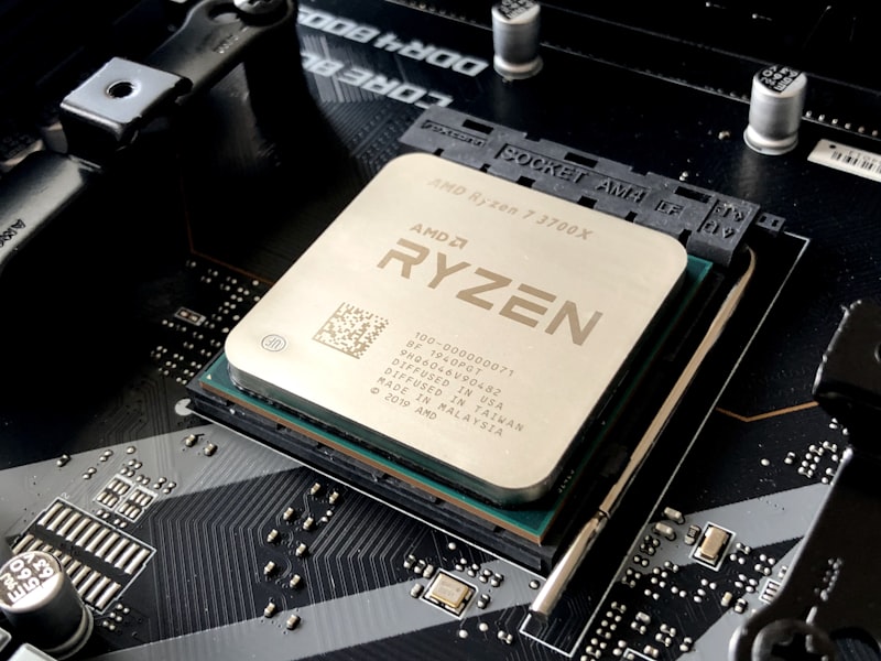
FPGAs offer two routes. Hard memory controllers are vendor-provided blocks (e.g., DDR4/LPDDR4 hard IP in modern AMD/Intel/Altera and Lattice devices) with a hardened PHY in the I/O ring — these reach the device's rated DDR speed and consume little fabric. Soft controllers are RTL mapped into the fabric with a soft-logic PHY using the SerDes/IO primitives; they are maximally flexible and portable but are limited by fabric timing closure and typically run slower, with heavy LUT/FF/BRAM usage. Use hard IP when the device has it and you want performance; use soft controllers for legacy DDR generations, unusual configurations, or devices lacking hard blocks. Expect timing-closure effort and routing constraints either way.
Automotive
Automotive controllers must satisfy ISO 26262 functional safety up to the ASIL level the application demands. This means end-to-end ECC (SECDED on the data path and increasingly in-line ECC that protects standard non-ECC LPDDR by stealing storage for check bits), data poisoning, address/command parity, safety mechanisms with documented diagnostic coverage, and robust error reporting to a safety manager. Devices are qualified to AEC-Q100 temperature grades (Grade 2 up to 105 C, Grade 1 up to 125 C, Grade 0 up to 150 C) and the memory is typically LPDDR4/LPDDR4X or LPDDR5 for its power and temperature behavior. Reliability, FIT-rate budgeting and a safety manual (FMEDA) accompany the IP. Choose an automotive-grade controller when a memory fault could affect a safety goal (ADAS, braking, cluster).
Aerospace / Defense
Space and defense add the radiation environment. Single-event upsets (SEU) flip bits and single-event functional interrupts (SEFI) can hang a device, so the controller needs EDAC (error detection and correction, commonly SECDED or stronger Reed-Solomon/BCH), background memory scrubbing to wash out accumulated upsets before they become uncorrectable, and SEFI detection/recovery. Memory choice favors rad-hard or rad-tolerant parts; many space designs still prefer SDR/DDR/DDR2/DDR3 SDRAM over the latest DDR5 because mature, rad-characterized parts exist, the simpler PHY is easier to make robust, and derating margins are generous. Longevity and obsolescence management (10-25 year missions) and component derating dominate the decision — not peak bandwidth. Choose rad-tolerant controllers with configurable EDAC and scrubbing for any orbital or high-altitude/defense system.
| Criterion | ASIC | FPGA | Automotive | Aerospace / Defense |
|---|---|---|---|---|
| Typical DDR gen | DDR5 / LPDDR5X | DDR4 / LPDDR4 (hard IP) | LPDDR4/4X / LPDDR5 | DDR2/DDR3 SDRAM (rad-hard) |
| Controller type | Hardened ctrl + DFI PHY | Hard IP or soft RTL | Safety-certified ctrl + PHY | Rad-tolerant ctrl + EDAC |
| Key priority | PPA / peak performance | Flexibility / time-to-market | Functional safety (ASIL) | Reliability / longevity |
| Safety / reliability | Optional ECC | Optional ECC | ISO 26262, in-line ECC, AEC-Q | EDAC, scrubbing, SEU/SEFI mit. |
| Cost model | High NRE, low unit @ volume | Low NRE, high unit | High (qual + safety docs) | Very high (low volume, screening) |
| Time-to-market | Longest (tape-out) | Fastest (reprogrammable) | Long (certification) | Longest (qual + radiation test) |
Selection Flowchart
Use the decision flow below as a first-order filter. Start from the platform, weigh performance against flexibility, layer in safety/reliability, then size ranks, capacity and port count.
Peak Bandwidth Calculation
Peak theoretical bandwidth is a simple, essential sanity check that depends only on the transfer rate and the bus width. ECC bits do not add usable payload bandwidth, so compute with the data width (64 bits = 8 bytes for a standard channel).
Peak DDR Bandwidth
BW = data_rate (MT/s) x bus_width (bytes)
DDR double-pumps the clock, so data_rate (MT/s) = 2 x clock (MHz). A 64-bit channel is 8 bytes wide.
- DDR4-3200, x64: 3200 MT/s x 8 B = 25.6 GB/s per channel
- DDR5-6400, x64: 6400 MT/s x 8 B = 51.2 GB/s per channel
- LPDDR5-6400, x32 sub-channel: 6400 MT/s x 4 B = 25.6 GB/s per sub-channel
Effective (sustained) bandwidth is lower — typically 60-85% of peak — after refresh (tRFC), read/write turnaround, activate/precharge overhead and row-buffer misses. This efficiency gap is exactly what the multi-port scheduler works to minimize.
Implementation Best Practices
- Lock the PHY training sequence first: bring up write leveling, read DQS-gate training and per-bit deskew before chasing performance; most "controller" bugs are really training/calibration issues at the DFI boundary.
- Enable ECC appropriately: use side-band ECC where the DRAM supports it, or in-line ECC on non-ECC LPDDR for automotive/reliability targets; wire correctable/uncorrectable error reporting to your safety manager.
- Floorplan the PHY against the pad ring: keep DQ/DQS byte lanes short and length-matched, give the PHY clean supplies and ground reference, and respect the vendor's keep-out for best signal integrity.
- Match DFI versions: confirm the controller and PHY implement the same DFI revision and the same clock ratio (1:1 / 1:2 / 1:4), and co-verify the update/low-power handshakes.
- Tune QoS deliberately: give isochronous (display) and latency-critical (CPU) traffic bounded latency via priority and bandwidth regulators; let GPU/NPU soak the remainder. Validate under worst-case concurrent traffic.
- Choose the page policy to match traffic: open-page for locality-rich streams, close/adaptive-page for random multi-master traffic; measure row-buffer hit rate on real workloads.
- Budget for signal integrity on multi-rank channels: de-rate the data rate as ranks and loading increase, and use ODT/DBI settings the PHY characterization recommends.
- Plan scrubbing and derating for aerospace: size the scrub interval against the expected upset rate so no word accumulates two errors before a scrub, and derate voltage/temperature per mission profile.
Conclusion
Choosing a DDR controller is a systems decision, not a datasheet lookup. First master the hierarchy — channels, ranks (and their chip selects), bank groups, banks, rows and columns — because it drives capacity, timing and signal integrity together. Then size the controller to its platform: ASIC for peak PPA, FPGA for flexibility and time-to-market, automotive for ISO 26262 safety with ECC and AEC-Q grades, aerospace for EDAC, scrubbing and radiation tolerance. Underneath all four, the DFI interface cleanly separates your reusable controller RTL from the hardened PHY, and a well-tuned multi-port scheduler turns raw peak bandwidth into sustained, QoS-honoring throughput.
Vcores offers silicon-proven DDR2/DDR3/DDR4/DDR5 and LPDDR memory controller IP with multi-port arbitration, DFI-compliant PHY integration, configurable ECC/EDAC, comprehensive verification, and expert support for ASIC, FPGA, automotive and aerospace applications.