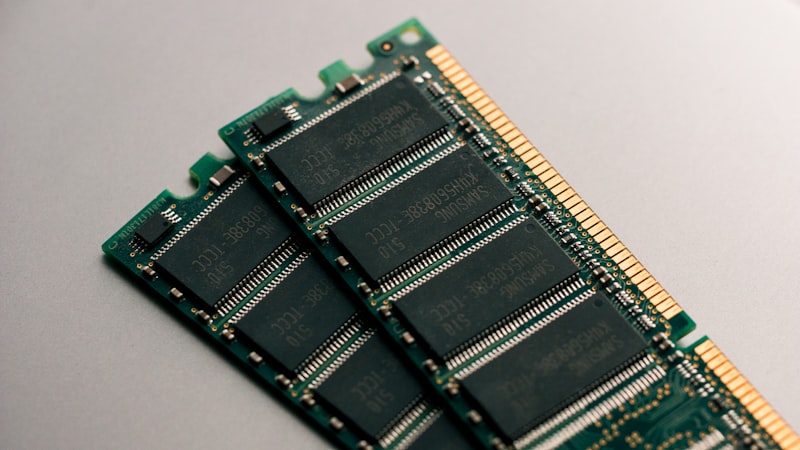
DDR5: The Next Generation Memory Standard
DDR5 SDRAM represents a significant leap forward in memory technology, offering doubled bandwidth, improved power efficiency, and enhanced reliability features compared to DDR4. This comprehensive guide examines the key differences between DDR5 and DDR4, helping system architects make informed decisions for their designs.
DDR5 vs DDR4 Quick Comparison
| Specification | DDR4 | DDR5 |
|---|---|---|
| Data Rate | 1600-3200 MT/s | 3200-8800 MT/s |
| Prefetch | 8n | 16n |
| Bank Groups | 4 | 8 |
| Burst Length | 8 | 16 |
| Operating Voltage | 1.2V | 1.1V |
| Channels per DIMM | 1 (64-bit) | 2 (32-bit each) |
Key Architectural Changes in DDR5
1. Dual-Channel Architecture
DDR5 fundamentally changes the memory channel architecture:
- DDR4: Single 64-bit channel per DIMM
- DDR5: Two independent 32-bit channels per DIMM
- Each channel operates independently with its own command/address bus
- Improves memory access efficiency for multi-threaded workloads
DDR4 DIMM Architecture:
┌─────────────────────────────────────────────────────────┐
│              Single 64-bit Data Channel                 │
│  ┌─────────┬─────────┬─────────┬─────────┬─────────┐   │
│  │ Rank 0  │ Rank 0  │ Rank 0  │ Rank 0  │ Rank 0  │   │
│  │ DRAM    │ DRAM    │ DRAM    │ DRAM    │ DRAM    │   │
│  └─────────┴─────────┴─────────┴─────────┴─────────┘   │
│              ↑ Single Command/Address Bus               │
└─────────────────────────────────────────────────────────┘

DDR5 DIMM Architecture:
┌─────────────────────────────────────────────────────────┐
│  Channel A (32-bit)     │     Channel B (32-bit)        │
│  ┌─────────┬─────────┐  │  ┌─────────┬─────────┐       │
│  │  DRAM   │  DRAM   │  │  │  DRAM   │  DRAM   │       │
│  └─────────┴─────────┘  │  └─────────┴─────────┘       │
│        ↑ CA Bus A       │        ↑ CA Bus B            │
└─────────────────────────────────────────────────────────┘
2. On-Die ECC (ODECC)
DDR5 introduces mandatory on-die error correction:
- Each DRAM device performs internal ECC
- Corrects single-bit errors within the device
- Improves data integrity without system ECC overhead
- Enables higher density dies with acceptable error rates
3. Decision Feedback Equalization (DFE)
DDR5 adds DFE for improved signal integrity at high speeds:
- Compensates for inter-symbol interference (ISI)
- Enables reliable operation at 6400+ MT/s
- Programmable tap coefficients
4. Power Management IC (PMIC)
DDR5 moves voltage regulation onto the DIMM:
- 12V input power from motherboard
- PMIC generates VDD (1.1V) and VDDQ locally
- Improved power efficiency and noise immunity
- Enables finer-grained power management
DDR5 Memory Controller Design Considerations
Training Requirements
DDR5 requires more extensive training compared to DDR4:
- Write Leveling: Per-byte DQS alignment
- Read Training: DQS-to-DQ centering
- Write Training: DQ-to-DQS alignment
- CA Training: Command/Address timing
- CS Training: Chip select timing (new in DDR5)
- DFE Training: Equalization coefficient optimization
Timing Parameters
| Parameter | DDR4-3200 | DDR5-4800 | DDR5-6400 |
|---|---|---|---|
| tCK (clock period) | 0.625 ns | 0.416 ns | 0.312 ns |
| tRCD (RAS to CAS) | ~14 ns | ~14 ns | ~14 ns |
| tRP (Precharge) | ~14 ns | ~14 ns | ~14 ns |
| tRAS (Active time) | ~32 ns | ~32 ns | ~32 ns |
| CL (CAS Latency) | 22 | 34 | 46 |
Refresh Management
DDR5 introduces new refresh options:
- Same Bank Refresh: Refresh one bank while accessing others
- Refresh Management (RFM): Mitigates row hammer attacks
- Fine Granularity Refresh: More flexible refresh scheduling
Bandwidth and Efficiency Comparison
Theoretical Peak Bandwidth
Bandwidth Calculation
Peak Bandwidth = Data Rate × Bus Width × Channels
- DDR4-3200 (1 DIMM): 3200 MT/s × 8 bytes = 25.6 GB/s
- DDR5-4800 (1 DIMM): 4800 MT/s × 8 bytes = 38.4 GB/s
- DDR5-6400 (1 DIMM): 6400 MT/s × 8 bytes = 51.2 GB/s
- DDR5-8800 (1 DIMM): 8800 MT/s × 8 bytes = 70.4 GB/s
Real-World Efficiency
DDR5's dual-channel architecture improves efficiency for:
- Multi-threaded applications with independent memory streams
- Smaller, more frequent memory accesses
- Workloads with high bank conflicts in DDR4
DDR4 to DDR5 Migration Guide
Controller IP Changes Required
- Dual-channel command/address interface
- 16n prefetch architecture support
- New mode register programming
- DFE training algorithm
- CS training support
- Updated refresh management
PHY Requirements
- Higher frequency operation (up to 4400 MHz)
- DFE receiver implementation
- Improved jitter performance
- Lower voltage signaling (1.1V VDD)
PCB Design Considerations
- Tighter trace matching for higher speeds
- 12V power delivery for PMIC
- Updated DIMM connector (288-pin, different key position)
Conclusion
DDR5 delivers substantial improvements in bandwidth, power efficiency, and reliability over DDR4. While the transition requires new controller IP and updated PHY designs, the performance benefits make DDR5 essential for next-generation computing platforms including servers, high-end desktops, and AI/ML accelerators.
Vcores offers DDR5 memory controller IP supporting speeds up to DDR5-6400, with comprehensive training algorithms, dual-channel support, and JEDEC compliance. Our IP includes configurable options for different application requirements from embedded to enterprise.